Quantum-π’s aim is i) to provide sub nanometer and nanoradian dimensional metrology tools to enable nanotechnology growth and benefit the microelectronics industry and ii) to develop new NEMS sensors superior in accuracy, smaller in size and of lower cost than existing ones.
Two specific type of products are:
sub-nanometer position metrology
nanoTrek® devices for the high-end
microelectronic and scientific markets, and
accelerometers, gyroscopes and
vibration NEMS sensors for the oil & gas exploration, drilling and exploitation market.
Several companies are currently testing
our products in the USA, UK, Germany
and Singapore.
Planned nanoTrek® products include:
wireless networks of smart sensors
(motion detection, perimeter security);
sonobuoys (Navy);
vibration measurements (perimeter
security sensing, CD drives prototyping
& testing, ship building, air-foil testing,
building stability);
accelerometers and gyroscopes (inertial
guidance systems, missile guidance,
aviation, shipping and automotive);
image stabilization systems in optical
devices (infra-darkred, night vision, vehicle
mounted, cameras and video);
ultra sensitive microphones
(intelligence, medicine, mobile phones);
displacement and tremor sensors in
nuclear test monitoring, mining, mineral
exploration, geology, tectonics;
seismometers - early earthquake
warning systems, tsunami detection;
In comparison with existing advanced
MEMS sensors (N.B. NEMS sensors are
not yet on the market in any noticeable
numbers), Quantum-π devices:
provide an order of magnitude
improvement in precision of
measurement;
are smaller and weigh less (entire
sensor weighs less than 0.1 g and is
smaller than 1mm2 in area, whereas
the sensing part is only 20
micrometers in size - one fifth of a
diameter of a human hair);
are more robust: Quantum-π
nanoTrek® sensors will use less
power and will have higher output
signal for a given stimulus;
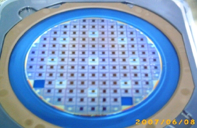
can be mass produced using
conventional semiconductor
manufacturing processes;
are cheaper,
will be incorporated in an intelligent
wired and wireless sensor networks.
The devices will have both commercial
(size, price) and technological
advantages (accuracy, resolution,
robustness) making them superior to
those currently available.
Products based on the technology have
the potential to supplant existing sensor
products in many applications and to
enable entirely new applications.
The operating principle of Quantum-π'snanoTrek® devices is quantum tunneling.
This makes them unique and advantageous over existing devices for
similar measurements which use techniques based on other physical principles (e.g. optical, interferometry,
capacitance, piezoelectricity etc.).
The only reported attempts to build quantum tunnelling sensors were based on a
cantilever tip-surface geometry. Such devices are inherently non-linear. Our
devices, on the other hand are linear and do not suffer from limitations such as restricted tip-to-plane movement.
Quantum-π's devices also have advantages over other type of devices, for example: